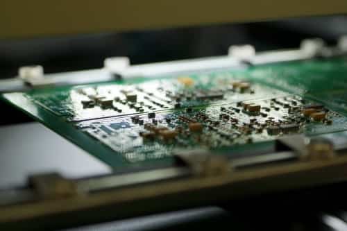
How Teddington has embraced the Surface Mount Technology PCB revolution
Teddington has produced assembled printed circuit boards (PCBs/PCBAs) since the 1960s. Back then, all the components were through hole, the solder was leaded, and the boards were cleaned with chemicals we’re no longer allowed to mention. As technology has advanced, and the environment has risen to the forefront of people’s collective consciousness, today’s PCBs bear no resemblance to their 20th century ancestors.
The dominant driving force behind this PCB revolution has undoubtedly been surface mount technology. It has dramatically altered the face of contract electronics manufacturing (CEM), particularly in terms of how PCBs are designed and laid out. The miniaturization of components and denser boards has sped up the production process, but component placing has forced companies to invest in new equipment. The smaller size of components also means visual inspections largely redundant – leading to further investment.

So how has Teddington adapted and responded to this constant re-examination of soldering techniques? Firstly, we have invested in our technology. Our Pick and Place and Automatic Optical Inspection (AOI) machines have either been replaced or updated to improve productivity and efficiency.
In particular, our AOI systems are some of the most powerful tools for ensuring industry-leading levels of accuracy and continuous process monitoring. They provide superior fault coverage – detecting component presence, polarity and component markings – and exceptional post reflow solder inspection capability.
Alongside traditional inspection techniques, such as visual inspections, functional tests and bed of nails circuit board test fixtures, this approach maintains quality while keeping customer costs to a minimum. In addition, both our Pick and Place and AOI machines are programmable from the same BOM supplied by customers for purchasing, so the same program is used more than once throughout the production process.
Through hole components are still used in production, but again technology has made the production and manufacture process much faster – saving our clients time and money. Setting up a selective solder cell allows an operator to populate the PCB while another PCB is being soldered, rather than having an operator constantly running boards through a flow solder machine as someone else populates them.
This also cuts down on the amount of flux being used as the selective solderer has a jet fluxer which only dispenses flux to each joint, and not the whole of the board, reducing the risk of flux residue and therefore preventing leakage currents which could disrupt electrical performance and electrochemical migration.
Fortunately, our efforts and investment have paid off. Today, through our process of continuous improvement, we have developed the ability to place, with total precision, thousands of components per hour, from 01005 packaged components to more expansive packages, according to IPC-A-610 standards.
We are fully equipped to undertake PCB batches from low to high quantities, and we constantly ensure a high level of placement accuracy and solder joint integrity is achieved throughout the process. Our ‘right first time’ attitude ensures greater productivity and flexibility – resulting in reliable, bespoke products of the highest quality.
So, however straightforward or complex your requirements, we are ready to help you today. Find out more about our CEM and PCBA services by clicking here or download our brochure.
Derek Pollitt, Production Manager at Teddington - connect with me on LinkedIn.

